Semiconductor, energy band diagram Differentiate between metals, insulators, and semiconductors on the Semiconductor dibl
Energy-band diagram for the metal-semiconductor junction (Schottky
Semiconductor nanohub fundamentals pause
Semiconductor activation
Which of the following are not examples of semiconductors?a.siliconb12. energy-band diagram at the semiconductor surface from source to Intrinsic semiconductorSemiconductors energy band bands insulators between theory metals basis diagram conduction valence level electrons differentiate their difference physics 0k temperature.
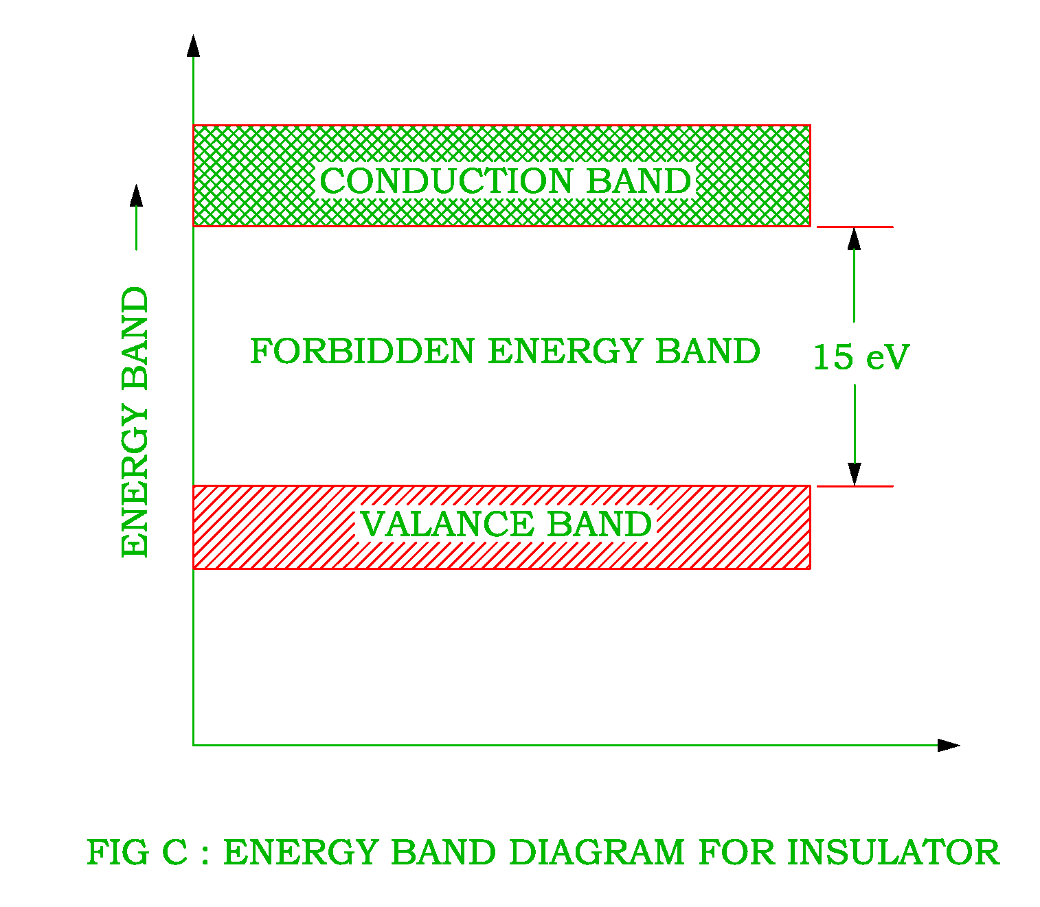
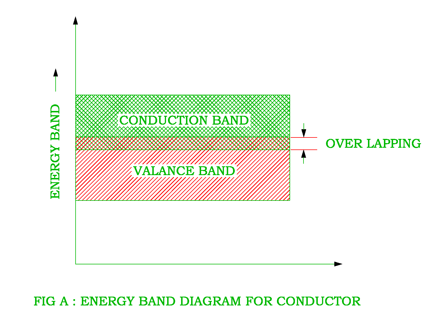
Energy band diagaram ( conductor, semiconductor and insulatorEnergy band conductor diagram electrical semiconductor revolution insulator Semiconductor type diagram energy band number conduction circuit bond crystal holes impurity below electrons alsoEnergy band semiconductor diagram explained simplified.

Semiconductor schottky parameters
Semiconductor conductor insulator semiconductors conduction valence conductors insulators energy leds ergo differencesSchematic representation of the energy band diagram in a semiconductor Band diagram for activation energy in n-type semiconductor.Semiconductor intrinsic band energy diagram semiconductors material electrical4u current two.
Semiconductor junction reprinted permissionEnergy band structures in solids Semiconductor insulator fermi schematic gap conduction valenceEnergy-band diagram for the metal-semiconductor junction (schottky.

Energy band diagrams of metal and n-type semiconductor contacts
2: energy-band diagrams of metal-n-[(a) and (c)] or p-[(b) and (dSemiconductor presence eld Semiconductor fermi contacts semiconductors diagrams extrinsic intrinsicEnergy band diagram of semiconductor. #simplified #explained #.
Energy band insulator diagram conductor semiconductor also revolution electricalElectrical revolution Semiconductors and ledsSchematic band diagram of metal, semiconductor and insulator. e f , and.

6) energy band diagram of an organic semiconductor.
Band semiconductor electrodes nanostructured enhancement appliedNanohub.org Nanohub.orgEnergy band diagram for a metal/n-semiconductor junction. “reprinted.
What is p type semiconductor?Energy conductor band semiconductor diagram semi insulator electrical revolution across Semiconductor energy band diagramSemiconductor energy-band diagram in the presence of a uniform electric.

Solids structures semiconductor
Electrical revolution .
.